In part 1 of this series we took a very quick tour through the whole process of designing a product. We will now begin a much more detailed look at designing a Digital Input/Output interface for a Z80 computer.
We start by stating what our goal is:
This project is the design of a digital input/output interface for a Z80 computer, culminating in the production of a printed circuit board for the RC2014 bus.
While the RC2014 bus is being used in this example, the basic design could be used on almost any Z80 system.
Our detailed specification for the project is this:
The product will be an RC2014 module, compatible with both the standard and the enhanced bus.
The module will provide 8 digital output lines and 8 digital input lines. Each input and output line will have an LED to show its state. Input and output signals will be available on a pin header for external connection.
The module’s I/O address will be configurable with jumpers, allowing it to be set to any address from 0x00 to 0xFF. It will only occupy one port address.
The design will allow many of these modules to be used at the same time.
To ensure the module is easy to use, there will be no requirement to initialise it. Only a single input or output instruction with be required to perform a read or a write.
Input and outputs will be compatible with 5 volt 74HCT series chips.
Block diagram
We start with a simple block diagram of the electronics.
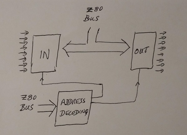
The specification calls for 8 inputs and 8 outputs, so we draw a block for each of these.
We also need address decoding to enable the input and output ports at the correct times, so we draw a block for this.
The address decoding controls the input and output ports, so we draw a line between the address decoding block and the input block and another line between the address decoding block and the output block.
The module is to be used on an RC2014 bus so we indicate this on the diagram. As the design is suitable for almost any Z80 system and the RC2014 bus is essentially a Z80 bus, I’ve labelled the bus “Z80 bus”.
The bus connects to the input block so the Z80 processor can read data from the inputs. Similarly, it connects to the output block so the Z80 processor can write data to the outputs. The bus also connects to the address decoding block as this block must determine when the Z80 wants to read from the inputs or write to the outputs.
Circuit diagram
We now need to draw a circuit diagram. We do this in manageable chunks by considering one block at a time, but first we need to understand enough about the workings of the Z80 bus.
The Z80 data book describes input and output operations in detail with the aid of this complex looking timing diagram.
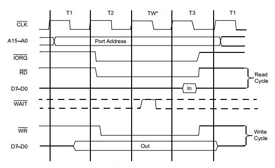
The diagram shows what happens on each signal, or signal type, during an input and an output cycle.
At this stage the important details on this diagram are the relationship between the address lines, the data lines, and the control signals IORQ (input/output request), RD (read) and WR (write). I’ve isolated these below for the write cycle and the read cycle.
The write cycle
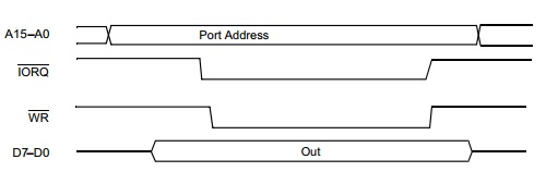
We can see that an output write occurs in this order:
- The port address is output on the address bus
- The data is output on the data bus
- The IORQ control signal goes low
- The WR control signal goes low
- The IORQ and WR signals go high
- The data bus goes tri-state
- The address bus changes (to read the next program instruction)
When writing to our module’s output port, the port address will be output on A0 to A7 and the required state of each of our module’s output bits will be on D0 to D7.
The read cycle
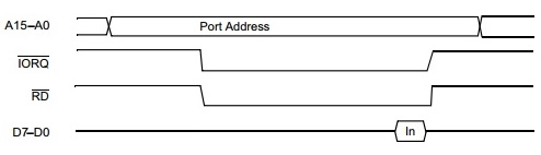
An input read occurs in this order
- The port address is output on the address bus
- The IORQ control signal goes low
- The RD control signal goes low
- The port device outputs its data on to the data bus
- The IORQ and RD signals go high
- The data bus goes tri-state
- The address bus changes (to read the next program instruction)
When reading from our module’s input port, the port address will be output on A0 to A7 and our module will output its data on D0 to D7.
Address decoding
Our block diagram shows the address decoding block providing a control signal to the output block and another signal to the input block.
From the simplified timing diagrams above, it can be seen that:
- The control signal to our module’s output block will need to be active when our module’s address is present on the address bus and the IORQ signal is low and the WR signal is low.
- The control signal to our module’s input block will need to be active when our module’s address is present on the address bus and the IORQ signal is low and the RD signal is low.
Notice that the only difference between the two control signals we need to generate is the RD and WR signals. Both control signals are active when our module’s address is present on the address bus and the IORQ signal is low. This gives us a strong hint that we need to first generate a signal when our module’s address is present on the address bus and the IORQ signal is low, and then use RD and WR to determine if we send an active control signal to the input block or the output block.
The first stage needs to compare the address on the address bus (A0 to A7) with our module’s address (as set with jumpers). For this we can use a comparator. We also need to ensure the signal generated is only active when IORQ is low.
Fortunately, the 74HCT688 was made for this very purpose. The 688 has two sets of 8 inputs which it constantly compares. If the two sets of inputs are the same and its enable signal is low, the 688 generates an active low output signal. Perfect. One set of inputs is the address bus A0 to A7, the other set is the 8 signals from the jumpers, and the enable signal is IORQ.
This gives us the circuit:
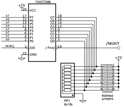
The value of the resistors in the resistor network is not critical. Anything between 1k and 100k should be fine. 10k is simply a convenient value which is low enough to give a good clean signal (immune from noise) and high enough not to waste unnecessary power.
The timing diagram for input or output to our module’s address is:
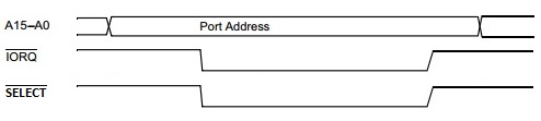
We now need to generate two versions of the SELECT signal: Read and write. The read version is when SELECT is active (low) and the processor’s RD signal is active (low). The write version is when SELECT is active (low) and the processor’s WR signal is active (low).
This can be achieved with simple OR gates. If either input is high (inactive) the output is high (inactive). If both inputs are active (low) the output is active (low).
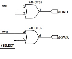
You may have heard warnings about the danger of ignoring the Z80’s M1 signal when decoding I/O addresses. In this case it can be safely ignored as we combine the address select signal with RD and WR. If you do not include RD and WR in the decoding circuit you usually need to instead ensure M1 is high to avoid getting unwanted I/O select signals when interrupts occur. For a full explanation see the Z80 data book.
In the next exciting instalment we will complete the circuit diagram.

These posts are great. Learning a lot. Thanks!